Audio Amplifier 200-500W
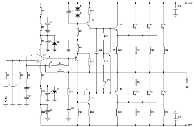
This high-power audio amplifier uses multiple complementary transistors in the output and driver stages to deliver robust audio output. The design can achieve power levels between 200 W and 500 W depending on load and supply.
Transistor Configuration
- T2: MJE15031 (NPN)
- T3, T4: MJE15030 (PNP)
- T5: MJE15031 (NPN)
- T6: BD139 (driver stage)
- T7–T12: MJ15003 (power output transistors, 4 per channel for left and right)
Power Output
Using 4 × MJ15003 per channel, the amplifier can provide a continuous output of 200 W–500 W into suitable speaker loads (typically 4 Ω or 8 Ω). The exact power depends on the power supply voltage and load impedance.
Power Supply
The amplifier requires a symmetrical high-current power supply with adequate voltage and current rating to feed the push-pull stages. A regulated ±50V to ±60V DC supply is typical for maximum output. Include proper smoothing and decoupling capacitors to minimize ripple.
Construction Notes
- Mount all MJ15003 output transistors on a large heatsink with thermal compound; each channel uses 4 output transistors for current sharing.
- Driver transistors (MJE15030/MJE15031 and BD139) should also be heatsinked or thermally coupled as needed.
- Keep input and feedback wiring short and separate from high-current output traces to avoid oscillations.
- Use adequate fusing and protection in the power supply due to high current levels.
- Check biasing and thermal tracking to prevent crossover distortion and thermal runaway in the output stage.
Key Features
- High-power output: 200–500 W RMS
- Complementary push-pull design for low distortion
- Multiple output transistors for high current capability
- Suitable for 4 Ω and 8 Ω speakers
- Robust driver stage with MJE15030/MJE15031 and BD139
Components
| Resistors | Capacitors | Semicondutor |
|---|---|---|
| R1 = 5k6 R2 = 33k R4 = 2k7 R5 = 33k R8 = R9 = 100Ω R12 = 150Ω R13 = 27k R14 = 1k5 R15 = 470Ω R16 = 68Ω R17 = 27k R18 = 68Ω R19 = 1k R20 = 470Ω R21 = R22 = 68Ω R25 - R29 = R23 - R24 |
C1 = 220n (470n) C9 = 100uF/63v |
T1 = BD 140 T2 = MJE 15031* T3 = MJE 15030* T4 = MJE 15030* T5 = MJE 15031* T6 = BD 139 T7 – T12 = MJ 15003 TP1 = 470Ω IC1 = TL 071 Z1 = Z2 =15v D1 = D2 = DUS |
| Power | Transistor | R6,R7,R10,R11 | R23 - R24 | R3 |
|---|---|---|---|---|
| 200W | 4x MJ 15003* | 3k3/0,25w | 0,27Ω/5W | 820 Ω |
| 300W | 4x MJ 15003 | 4k7/0,25w | 0,12 Ω/5W | 680 Ω |
| 400W | 6x MJ 15003 | 5k6/0,25w | 0,18 Ω/5W | 560 Ω |
| 500W | 8x MJ 15003 | 5k6/0,25w | 0,22 Ω/5W | 470 Ω |
Amplifier Power Supply
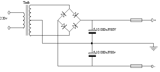
| Power / Out Impedance | Transformer | Power Transf | Elect. Capacitor |
|---|---|---|---|
| 200w/4 Ω | 2x36v | 300w | 2x10.000uF/80v |
| 300w/4 Ω | 2x44v | 400w | 2x15.000uF/80v |
| 400w/4 Ω | 2x49v | 550w | 2x20.000uF/100v |
| 500w/4 Ω | 2x54v | 650w | 2x20.000uF/100v |
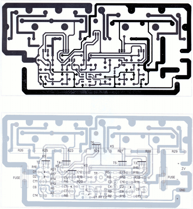
PCB
This pcb isn't in real scale, be carefull